
- 15 publications
- 60+ citations
- 8 features and highlights
- 100% collaborative
- 100% open access
- 13+ average impact factor
High Performance Fully Solid-State Electrochemically Exfoliated WS2 Transistor
Fatemeh Khorramshahi, Finn Huonder, Tian Carey, Jonathan Coleman, Tawfique Hasan
2026 10th IEEE Electron Devices Technology & Manufacturing Conference (EDTM), 1–3. Link to article and accepted manuscript (open access).
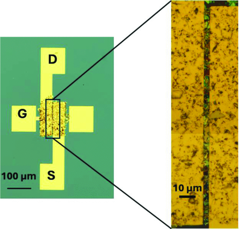 Electrochemical exfoliation (ECE) of transition metal dichalcogenides (TMDCs) yields large-area flakes suitable for low-temperature, scalable, solution-based deposition. This offers substrate-independent thin-film fabrication, unlike mechanically cleaved flakes or chemical vapor deposition (CVD) films that rely on substrate-specific growth and require additional transfer steps. However, producing high-performance, fully solid-state field-effect transistors (FETs) from such solution-processed materials remains challenging. In particular, uniform surface, continuous coverage and low-resistance interflake junctions are essential for clean interfaces. Residual contaminants from solution processing further degrade these interfaces and limit device performance, slowing progress toward reliable solid-state FETs derived from ECE-based TMDCs. While earlier solution-processed WS2 devices have shown promising characteristics, contact resistance and surface impurities often restrict their performance. Here we demonstrate fully solid-state WS2 transistors fabricated from ECE-derived flakes. Under ambient conditions and in the dark, the devices reach a field-effect mobility of ~10 cm2/V·s, an on/off ratio of ~105, and a subthreshold swing of ~190 mV/dec, values comparable to conventional solid-state implementations. Our work highlights the immense potential of ECE-derived TMDCs for large-area electronics.
Design Strategies and Emerging Applications of High-Performance Flexible Piezoresistive Pressure Sensors
Feng Luo, Artur Ciesielski, Paolo Samorì
Adv. Funct. Mater., 2026, 36, e75473. Link to article (open access).
Featured in Hot Topic: Wearable Sensors.
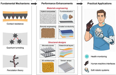 Flexible piezoresistive pressure sensors have become a keystone in emerging flexible and wearable electronic systems due to their mechanical compliance, high sensitivity, and scalable device architecture. These characteristics enabled rapid technological advances in continuous health monitoring, human–machine interfaces, soft robots, and electronic skin. Despite the considerable achievements, attaining simultaneously high sensitivity, stability, and reliability under realistic operating conditions remains challenging, requiring a unified materials- and structure-driven design paradigm. To address these challenges, this review establishes a systematic, mechanism-to-application roadmap for high-performance piezoresistive sensors. We discuss key performance metrics and fundamental sensing mechanisms, including contact resistance modulation, quantum tunneling, and percolation effects, which collectively govern the piezoresistive response. Linking these underlying physical mechanisms to macroscopic performance, we elaborate two central strategies to enhance performance: (i) materials engineering, including hybrid conductive composites, interfacial functionalization, porosity modulation, and graded multilayer designs; (ii) structural engineering like leveraging surface microstructuring, hierarchical layering, and three-dimensional conductive networks. The synergistic coupling of these strategies is illustrated through representative devices enabling health diagnostics, tactile feedback, and intelligent robotic systems. Finally, we discuss challenges and propose future research directions, including multi-modal sensing integration and on-chip intelligence, which are expected to drive the next generation of flexible electronics.
Laser-Assisted Phase Engineering of 2D MoS2 for Efficient Solution-Processed Electronics
Anna Zhuravlova, Minjuan Li, Osamah Alharbi, Yeonsu Jeong, Bin Han, Lei Gao, Mischa Bonn, Mario Lanza, Sheng Yang, Antonio Gaetano Ricciardulli, Paolo Samorì
Adv. Mater., 2026, in press (open access).
 Phase engineering of two-dimensional transition metal dichalcogenides (2D TMDs), such as MoS2, offers a powerful route for creating in-plane metal-semiconductor heterostructures and engineering low-resistance contacts in 2D electronics. Conventional strategies typically rely on chemically converting the semiconducting 2H phase into the metallic 1T/1T′ polymorph, a multistep process prone to incomplete phase conversion. Local laser-induced transition of 1T/1T′ into 2H MoS2 offers a facile one-step alternative. However, employing this approach to engineer patterned electronic devices has remained elusive. Here, we demonstrate laser-assisted 1T′→2H phase patterning in phase-pure, solution-processed MoS2, revealing the critical effect of irradiation atmosphere on phase transition. Although treatments in both ambient and inert environments produce apparent 2H Raman signatures, only inert-atmosphere irradiation yields micron-scale 2H domains within the 1T′ lattice. Leveraging this controlled transition, we fabricate field-effect transistors with laser-patterned 1T′–2H–1T′ lateral contacts that exhibit improved charge injection, as evidenced by order-of-magnitude higher mobility and ION/IOFF ratio, reduced hysteresis, and a ∼30% lower effective Schottky barrier height compared with conventional Au-2H contacts. These findings establish a robust and scalable route for functional laser-induced phase conversion in MoS2 and provide a practical strategy for efficient and seamlessly integrated 2D electronic devices and circuits.
Site-selective functionalization of solution-processed transition metal dichalcogenides for vertical and lateral covalent networks and heterostructures
Anna Zhuravlova, Paolo Samorì, Antonio Gaetano Ricciardulli
Nanoscale, 2026, 18, 9574–9582. Link to article (open access).
Featured in Nanoscale 2026 Emerging Investigators and Recent Review Articles.
 Covalent chemistry provides a robust route to functionalize transition metal dichalcogenides (TMDs), endowing them with new properties and enabling control over their interfaces. This minireview surveys covalent functionalization strategies for TMDs, emphasising site-selectivity and preferential binding to the basal plane or at the edges. It also discusses how these reactions enable the formation of covalently interconnected vertical heterostructures and lateral percolated homo- and heteronetworks, which can be assembled directly from TMD inks. We highlight emerging examples of such covalent 2D–2D architectures and outline challenges and opportunities in scalable covalent homo- and heterostructures fabrication featuring solution-processed TMDs.
Composition-Dependent Wide-Range Tunability of Optical and Electronic Properties in SnSxSe(2-x) Alloy Nanosheets
Nicolas J. Diercks, Rebekah A. Wells, Shixin Liu, Tian Carey, Jack Doran, Joseph Neilson, YeonJu Kim, Jun-Ho Yum, Goutam Ghosh, Hannah Johnson, Laurens D. A. Siebbeles, Jonathan N. Coleman, Kevin Sivula
Small, 2026, 22, e12066. Link to article (open access).
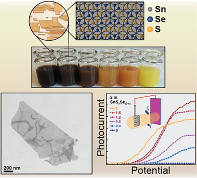 Isovalent alloying in printable metal dichalcogenide nanomaterials enables precise, application-targeted property tuning. However, a scalable platform offering broad optical and electrical tunability has so far remained elusive. Herein, we establish a powder-based, solution-processed route to access the full domain of SnSxSe(2-x) alloy nanosheets, providing control over a wide range of properties through chalcogenide composition. The n-type nanosheet alloy series shows a wide spread in optical and in-plane electrical properties, ranging from 1.67 eV and low bandgap metallic-like behavior for 2D SnSe2, to 2.46 eV and wide bandgap semiconducting behavior with high-resistivity for 2D SnS2. The out-of-plane conductivity is also tunable, showing nonmonotonic behavior with an optimal chalcogenide ratio of x = 1.2 – 1.6. Using photoelectrochemistry as an example, we highlight how the interplay of these tunable properties enables optimized performance for targeted applications. The exceptional range of tailorable properties reported here provides a roadmap for tuning these alloys, thereby opening avenues for their potential application in a multitude of fields.
Imaging junctions in two-dimensional semiconductor nanosheet networks
Jelena Pešić, Simon Leitner, Joseph Neilson, Igor Stanković, Muhammad Zubair Khan, Dragana Tizić Matković, Adam G. Kelly, Tian Carey, Jonathan Coleman, Aleksandar Matković
npj 2D Mater. Appl., 2025, 9, 90. Link to article (open access).
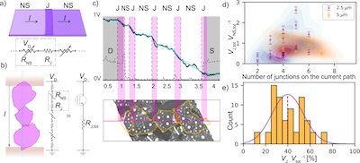 This study explores the challenges associated with translating electrical characteristics of individual two-dimensional semiconductor nanosheets into a network of partially overlapping sheets. Such systems typically suffer from high-energy barriers required to overcome the junctions formed between the adjacent nanosheets, and consequently quench the current passing through the network. We use in-operando Kelvin probe force microscopy to image electrostatic potential profiles during the operation of MoS2 nanosheet network transistors. Direct imaging of the potential drops allows us to distinguish contributions from individual nanosheets and those from junctions, correlated by the junction-related potential drops with the network morphology. A diagram-based model is developed to describe the system numerically and to estimate the current path formation probabilities. Finally, a correlation with the integral electrical characteristics of the nanosheet-based transistors is made using a robust Y-function approach. It is shown that the total junction resistance is well estimated by the proposed equivalent circiut model.
Electronic properties and circuit applications of networks of electrochemically exfoliated 2D nanosheets
Tian Carey, Kevin Synnatschke, Goutam Ghosh, Luca Anzi, Eoin Caffrey, Emmet Coleman, Changpeng Lin, Anthony Dawson, Shixin Liu, Rebekah Wells, Mark McCrystall, Jan Plutnar, Iva Plutnarová, Joseph Neilson, Nicola Marzari, Laurens D. A. Siebbeles, Roman Sordan, Zdenek Sofer, Jonathan N. Coleman
Nat. Commun., 2025, 16, 9038. Link to article (open access).
Featured in Collection: Engineering the future of 2D transistors: scaling, p-doping, and contact strategies.
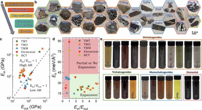 High aspect-ratio 2D materials are promising for solution-processed electronics, yet the factors controlling exfoliation remain unclear and relatively few solution-processed networks have been electrically characterized. Here we combine theory and experiment to show that electrochemical exfoliation of layered crystals with sufficient stiffness-anisotropy (in-plane/out-of-plane Young’s modulus ratio >1.7) yields high aspect-ratio nanosheets with intrinsic mobilities μNS = 20–75 cm²V⁻¹s⁻¹ across transition metal dichalcogenides and related alloys. Impedance spectroscopy indicates that solution-deposited networks can achieve junction-to-nanosheet resistance ratios (RJ/RNS) as low as ~3, supporting theoretical predictions that μNS/μNet = RJ/RNS + 1 and suggesting that further reductions in RJ will increase μNet toward the nanosheet limit (μNS). These networks display n-type, p-type, and ambipolar behaviour, with on/off ratios up to 10⁵ and mobilities μNet = 13 cm²V⁻¹s⁻¹. Here, we show that such high-performing 2D materials enable functional solution-processed circuits, including inverters, buffers, a 4-bit digital-to-analog converter, and a circuit capable of encoding and decoding 7-bit ASCII messages.
Solution-processed negative gauge factor PtSe2 strain sensors
Cansu Ilhan, Eoin Caffrey, Shixin Liu, Jose Munuera, Zdeněk Sofer, Iva Plutnarová, Michael A. Morris, Jonathan N. Coleman, Tian Carey
Nanoscale, 2025, 17, 18083–18091. Link to article (open access).
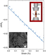 We undertake electrochemical exfoliation of a 2D semiconductor platinum diselenide, PtSe2 and investigate the piezoresistance response of a solution-processed network. Due to the large PtSe2 aspect ratios, exceeding 300, we achieve conformal flake-to-flake junctions and good inter-flake electrical coupling. Our measured piezoresistive gauge factor is negative (−5.45), consistent with the intrinsic negative gauge factor of PtSe2. This negative network gauge factor implies that strain is transferred from the substrate to the nanosheets. However, detailed modelling shows that the strain transferred to the nanosheets is much smaller than the applied strain, showing that conformal junctions do not necessarily lead to good mechanical coupling between nanosheets. Our model implies that this gauge factor is consistent with a strain transfer efficiency of 8.5%. Our strain sensor also demonstrated a cyclic response for over 1000 cycles, enabling the sensor to be used in future flexible optoelectronics applications.
Welding 2D Semiconducting Crystals by Covalent Stitching of Grain Boundaries in WS2
Bin Han, Chun Ma, Ke Jiang, Maria Batuk, Ahin Roy, Lucia Hughes, Hanlin Wang, Verónica Montes-García, Can Wang, Fanny Richard, Devu Prasad, Antonio Gaetano Ricciardulli, Sara Bals, Valeria Nicolosi, Yumeng Shi, Paolo Samorì
J. Am. Chem. Soc., 2025, 147, 24162–24170. Link to article and accepted manuscript (open access).
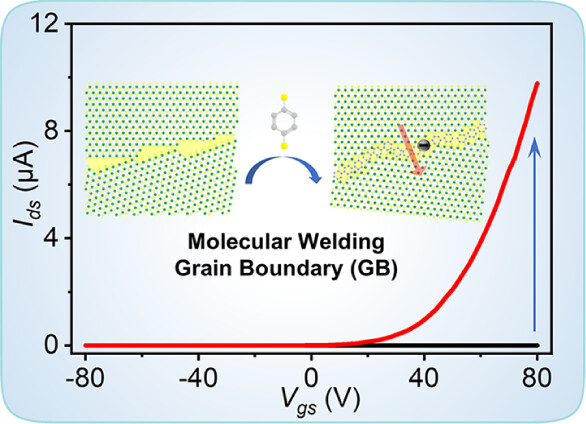 The advent of transition metal dichalcogenides (TMDCs) has revolutionized the field of optoelectronics. In this context, recent advances in the large-area synthesis of monolayer WS2 opened the door to potential optoelectronic applications because of its inherently high photoluminescence (PL) yield and superior electron mobility. However, randomly distributed point and line defects are key bottlenecks for efficient charge transport, hindering further development of system-on-chip (SoC) technologies. Herein, we report a molecular welding strategy using benzene-1,4-dithiol (BDT) to simultaneously passivate sulfur vacancies and bridge grain boundary (GB) fissures in monolayer WS2. The GB welding was monitored on the atomic scale by high-angle annular dark-field scanning transmission electron microscopy. This treatment yields uniform PL emission, ∼200-fold enhancement in electron mobility, and a three-order-of-magnitude increase in both on-state current and Ion/Ioff ratio for transistors across GBs, comparable to intragrain characteristics. Additionally, temperature-dependent PL spectroscopy was employed to identify the defect types and the activation energy of GBs. Our approach, utilizing the facile vapor deposition of ad-hoc molecules to repair line defects in 2D crystals, offers a scalable and effective solution to repair extended line defects in two-dimensional (2D) semiconductors, advancing the development of high-performance, uniform 2D optoelectronic systems.
Nonlinear Conductive Graphene Composites for Pressure Sensing with a Linear Response and Voltage-Driven Thermal Correction
Feng Luo, Artur Ciesielski, Paolo Samorì
Adv. Mater., 2025, 37, 2503867. Link to article (open access).
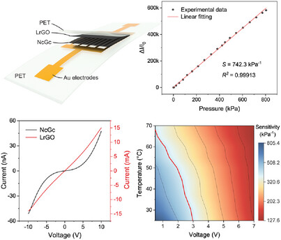 Thermal fluctuations pose a significant challenge to the signal stability of nanomaterial-based piezoresistive pressure sensors, limiting their effectiveness in applications such as electronic skin and robotics. Conventional temperature compensation strategies often rely on additional thermal sensors or complex calibration algorithms. Here, a flexible pressure sensor is reported featuring a nonlinear conductive graphene composite layer within a bilayer architecture, enabling bias voltage-controlled sensitivity without structural redesign. The sensor achieves ultra-high sensitivity (742.3 kPa−1), a broad linear sensing range of up to 800 kPa (R2 = 0.99913), and excellent long-term durability over 10 000 cycles. Crucially, the unique nonlinear characteristics enable the bias voltage to function as an internal remote control for correcting temperature drifts between 25 and 60 °C, as demonstrated by precise manipulation in robotic grippers under varying temperature conditions. This work offers a universal strategy for building environmentally adaptive sensors, advancing the development of robust and high-precision wearable electronics.
Carrier Multiplication and Photoexcited Many-Body States in Solution-Processed 2H-MoSe2
Goutam Ghosh, Tian Carey, Stevie Furxhiu, Sven Weerdenburg, Nisha Singh, Marco van der Laan, Susan E. Branchett, Sophie Jaspers, John W. Suijkerbuijk, Fedor Lipilin, Zdeněk Sofer, Jonathan N. Coleman, Peter Schall, Laurens D. A. Siebbeles
ACS Nano, 2025, 19, 10347–10358. Link to article (open access).
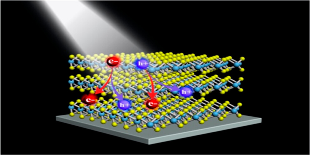 Carrier multiplication (CM), where a single high-energy photon generates multiple electron–hole pairs, offers a promising route to enhance the efficiency of solar cells and photodetectors.Transition metal dichalcogenides, such as 2H-MoTe2 and 2H-WSe2, exhibit efficient CM. Given the similar electronic band structure of 2H-MoSe2, it is expected to show comparable CM efficiency. In this study, we establish the occurrence and efficiency of CM in a solution-processed thin film of bulk-like 2H-MoSe2. We characterize the dynamics of excitons and free charge carriers by using ultrafast transient optical absorption and terahertz spectroscopy. At higher photon energy the efficiency is comparable to literature results for 2H-MoTe2 grown by chemical vapor deposition (CVD) or in bulk crystalline form. At higher photon energies the experimental CM efficiency is reproduced by theoretical modeling. We also observe CM for photon energies below the energetic threshold of twice the band gap, which is most probably due to subgap defect states. Transient optical absorption spectra of 2H-MoSe2 exhibit features of trions from which we infer that photoexcitation leads to free charge carriers. We find no signatures of excitons at the indirect band gap. From analysis of the frequency dependence of the terahertz conductivity we infer that scattering of charge carriers in our sample is less than for CVD grown or bulk crystalline 2H-MoTe2. Our findings make solution-processed 2H-MoSe2 an interesting material for exploitation of CM in photovoltaic devices.
Using Electrical Impedance Spectroscopy to Separately Quantify the Effect of Strain on Nanosheet and Junction Resistance in Printed Nanosheet Networks
Eoin Caffrey, Tian Carey, Luke Doolan, Anthony Dawson, Emmet Coleman, Zdeněk Sofer, Oran Cassidy, Cian Gabbett, Jonathan N. Coleman
Small, 2025, 21, 2406864. Link to article (open access).
 Many printed electronic applications require strain-independent electrical properties to ensure deformation-independent performance. Thus, developing printed, flexible devices using 2D and other nanomaterials will require an understanding of the effect of strain on the electrical properties of nano-networks. Here, novel AC electrical techniques are introduced to fully characterize the effect of strain on the resistance of high-mobility printed networks, fabricated from of electrochemically exfoliated MoS2 nanosheets. These devices are initially characterized using DC piezoresistance measurements and show good cyclability and a linear strain response, consistent with a low gauge factor of G ≈ 3. However, AC impedance spectroscopy measurements, performed as a function of strain, allow the measurement of the effects of strain on both the nanosheets and the inter-nanosheet junctions separately. The junction resistance is found to increase linearly with strain, while the nanosheet resistance remains constant. This response is consistent with strain-induced sliding of the highly-aligned nanosheets past one another, without any strain being transferred to the sheets themselves. The approach allows for the individual estimation of the contributions of dimensional factors (G ≈ 1.4) and material factors (G ≈ 1.9) to the total gauge factor. This novel technique may provide insights into other piezoresistive systems.
Graphene-Based Pressure Sensor Application in Non-Invasive Pulse Wave Velocity Continuous Estimation
Irene Buraioli, Stefania Vitale, Andrea Valerio, Alessandro Sanginario, Dario Leone, Sabrina Conoci, Artur Ciesielski, Alberto Milan, Danilo Demarchi, Paolo Samorì
Adv. Mater. Technol., 2025, 10, 2400876. Link to article (open access).
Featured in Advanced Materials Technologies Editors’ Choice, Hot Topic: Carbon, Graphite, and Graphene, and Hot Topic: Wearable Sensors.
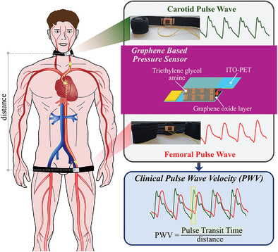
Monitoring the cardiovascular health of patients and early diagnosis of heart diseases are highly sought after as they can represent a true cornerstone in tomorrow's healthcare surveillance. Here, an unprecedented non-invasive device prototype is reported for pulse wave velocity (PWV) measurement based on a piezoelectric graphene pressure sensor. PWV is a critical health indicator that estimates arterial stiffness by measuring the velocity of arterial pulse flow through the circulatory system. The sensor incorporates advanced electronic components and data analysis tools, enabling the measurement of pulse transit time (PTT), that is the time required for the pulse wave to travel between carotid and femoral artery sites. Significantly, the outcomes obtained through the novel method, which involved monitoring 10 patients within clinical environment, show statistical similarity to results obtained using established technology for the PWV estimation such as SphygmoCor. In particular, the mean difference between measurements done with the two techniques resulted in 0.1 m s−1, that is <2%, underscoring the reliability of the novel device. The technology holds big promise for enhancing cardiovascular healthcare delivery: it is wearable, potentially exploitable by a non-expert user, and it needs to be powered with just 0.2 V, thus it can become compatible even with applications in point-of-care settings.
Reduced Graphene Oxide-Based Flexible Pressure Sensor for Biomedical Applications
Alessandro Sanginario, Irene Buraioli, Marco Boscherini, Stefania Vitale, Sabrina Conoci, Daniele Botto, Dario Leone, Alberto Milan, Artur Ciesielski, Paolo Samorì, Danilo Demarchi
IEEE Sens. J., 2024, 24, 37090–37103. Link to article (open access).
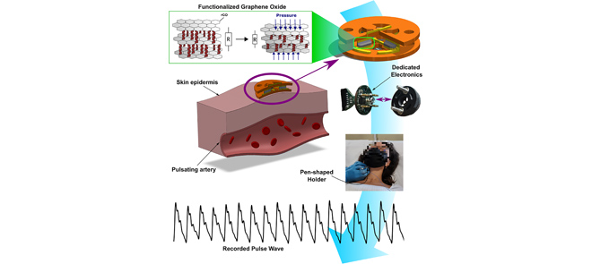 Pressure sensing is a crucial technique for various biomedical applications, where it can provide valuable information about the health and function of different organs and systems. This article reports the development of a novel integrated pressure sensor based on modified reduced graphene oxide (rGO), a graphene-derivative material with enhanced piezoresistive properties. The sensor is fabricated on a flexible printed circuit board (PCB) substrate and conditioned by a smart current-based Wheatstone bridge circuit, which enables high sensitivity, wide detection range, fast response and recovery, and good stability under cyclic loading. The sensor achieves a measured sensitivity of 0.281 kPa−1 (at 0.5 kPa load). A mechanical system is also designed to adapt the sensor to different anatomical sites and improve its elastic recovery. The sensor’s functionality is initially demonstrated through its response to controlled mechanical stimulation, achieving a signal-to-noise ratio (SNR) of 25 dB. Subsequently, in a practical application, physiological signals from the carotid and femoral arteries of volunteers were acquired. The system effectively captured the pulse waveforms with high fidelity and accuracy (23.5-dB SNR) and measured the pulse transit time, an important parameter for estimating the pulse wave velocity (PWV) and arterial stiffness. The sensor is not limited to this specific application and can be easily extended to other domains where pressure sensing is required. In conclusion, it offers a low-cost, flexible, and user-friendly solution for noninvasive biomedical monitoring and diagnosis.
Quantifying the effect of nanosheet dimensions on the piezoresistive response of printed graphene nanosheet networks
Eoin Caffrey, Jose M. Munuera, Tian Carey, Jonathan N. Coleman
Nanoscale Horiz., 2024, 9, 1774–1784. Link to article (open access).
Highlighted in Nanoscale Horizons Community Board Pick.
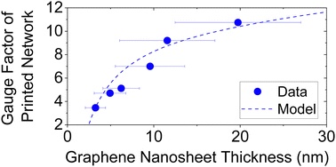 Printed networks of 2D nanosheets have found a range of applications in areas including electronic devices, energy storage systems and sensors. For example, the ability to print graphene networks onto flexible substrates enables the production of high-performance strain sensors. The network resistivity is known to be sensitive to the nanosheet dimensions which implies the piezoresistance might also be size-dependent. In this study, the effect of nanosheet thickness on the piezoresistive response of nanosheet networks has been investigated. To achieve this, we liquid-exfoliated graphene nanosheets which were then subjected to centrifugation-based size selection followed by spray deposition onto flexible substrates. The resultant devices show increasing resistivity and gauge factor with increasing nanosheet thickness. We analyse the resistivity versus thickness data using a recently reported model and develop a new model to fit the gauge factor versus thickness data. This analysis allowed us to differentiate between the effect of strain on inter-nanosheet junctions and the straining of the individual nanosheets within the network. Surprisingly, our data implies the nanosheets themselves to display a negative piezo response.
![]()